The van der Pauw method measures resistivity and Hall coefficient of thin, flat, and homogeneous materials using four-point contacts on the edges.
Introduction to the van der Pauw Method
The van der Pauw method is a widely-used technique for measuring the resistivity and Hall coefficient of a thin, flat, and homogeneous semiconductor material. Named after its developer, Leo J. van der Pauw, the method is particularly useful for materials with irregular shapes or unknown geometries.
Principle of the van der Pauw Method
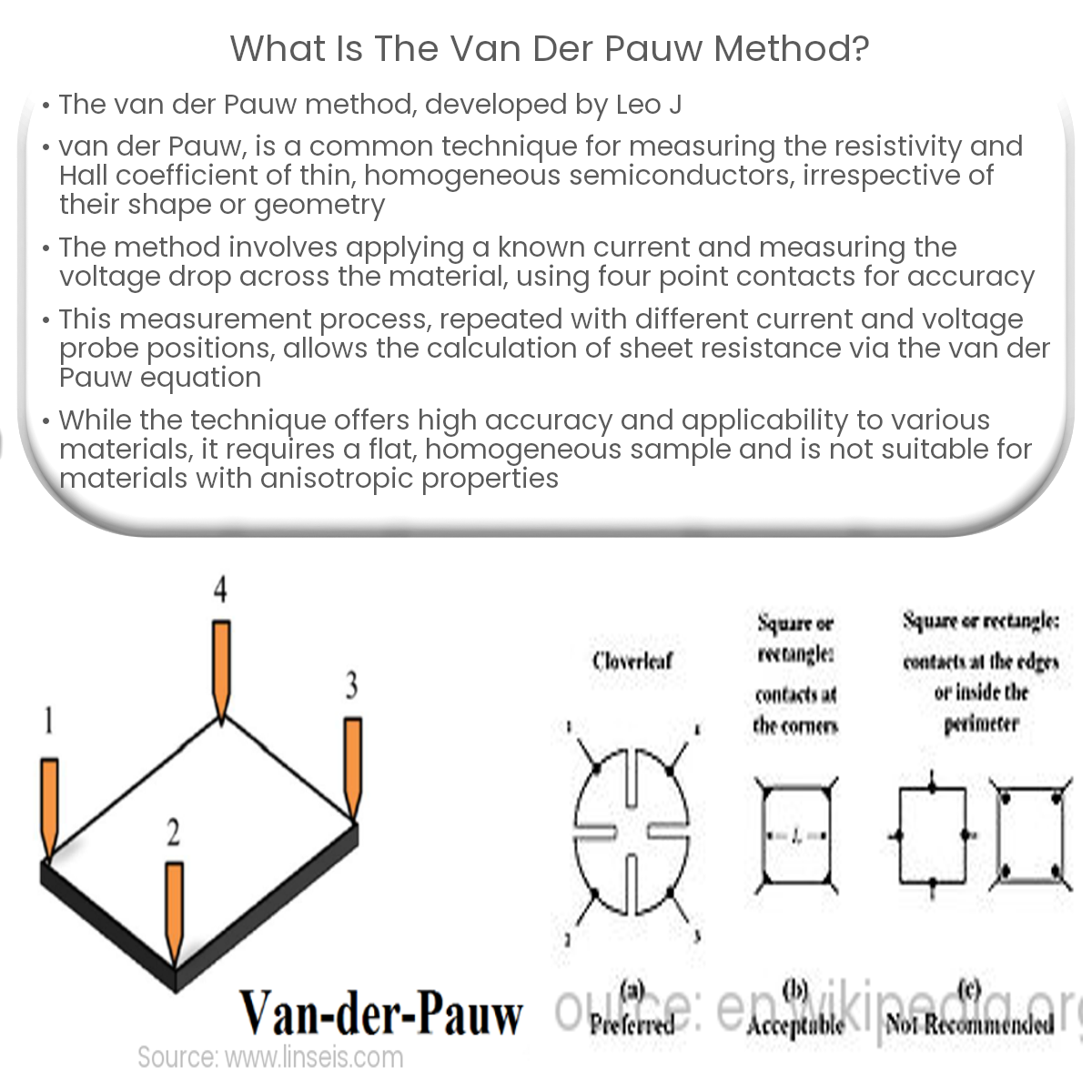
The van der Pauw technique is based on the principle that the resistivity of a material can be obtained by measuring the voltage drop across it when a known current is applied. The method employs four point contacts, placed on the edges of the sample, to minimize contact resistance effects and ensure accurate measurements.
Measurement Process
To perform the van der Pauw measurement, a constant current is applied between two opposite contacts on the sample, and the voltage difference between the other two contacts is measured. This process is repeated by changing the positions of the current and voltage probes until all possible combinations are tested.
By analyzing the recorded voltage drops and currents, the sheet resistance can be calculated using the van der Pauw equation:
Rs = πd(V1/I1 + V2/I2)/ln(2)
Where Rs is the sheet resistance, d is the sample thickness, V1 and V2 are the measured voltage drops, and I1 and I2 are the applied currents.
Advantages and Limitations
Some advantages of the van der Pauw method include:
- Applicability to samples with irregular shapes and unknown geometries
- Minimal influence of contact resistance
- High accuracy and reproducibility
However, there are some limitations to the technique:
- Requires a flat, homogeneous sample with negligible thickness variation
- Not suitable for materials with anisotropic properties
- May be affected by surface contamination and edge effects
Conclusion
The van der Pauw method is a versatile technique for characterizing the electrical properties of semiconductor materials. With proper sample preparation and accurate measurements, it offers reliable and precise results for various research and industrial applications.