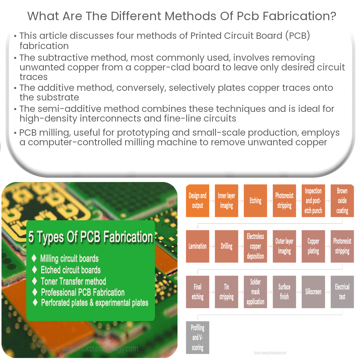
PCB fabrication methods include subtractive, additive, semi-additive, and PCB milling, each with different advantages and suited for specific projects.
Introduction
Printed Circuit Board (PCB) fabrication is the process of manufacturing PCBs that form the backbone of modern electronic devices. There are several methods available to produce PCBs, each with its advantages and drawbacks. This article will discuss the different methods of PCB fabrication, including:
1. Subtractive Method
The subtractive method is the most commonly used technique for PCB fabrication. It involves the removal of unwanted copper from a copper-clad board, leaving only the desired circuit traces. This process includes several steps:
- Photolithography: A photosensitive layer is applied to the copper-clad board, followed by exposure to UV light through a photomask with the circuit pattern.
- Etching: The exposed areas are chemically etched away, leaving only the desired copper traces.
- Drilling: Holes are drilled for through-hole components and vias to connect different layers.
- Plating: A thin layer of metal, usually copper, is deposited on the drilled holes to provide electrical connectivity between layers.
- Solder mask application: A protective layer is applied to prevent short circuits and protect the copper traces from oxidation.
2. Additive Method
In the additive method, the copper traces are selectively plated onto the substrate. This process involves:
- Substrate preparation: The substrate is cleaned and coated with a thin layer of metal, usually copper.
- Photolithography: The circuit pattern is transferred onto the substrate using a photosensitive layer and UV light exposure.
- Electroplating: Copper is electrochemically deposited onto the exposed areas, forming the circuit traces.
- Removal of the photosensitive layer: The remaining photosensitive layer is removed, leaving the copper traces on the substrate.
3. Semi-additive Method
The semi-additive method is a combination of the additive and subtractive methods. It involves the selective plating of copper traces followed by the removal of excess copper. This technique is ideal for high-density interconnects (HDI) and fine-line circuits.
4. PCB Milling
PCB milling, also known as mechanical etching or CNC routing, involves using a computer-controlled milling machine to remove the unwanted copper from the board. This method is suitable for prototyping and small-scale production, as it does not require chemicals or photolithography.
Conclusion
There are various methods for PCB fabrication, each with its advantages and drawbacks. The choice of fabrication method depends on factors such as the complexity of the design, the required level of precision, and production scale. Understanding these methods will help you make an informed decision when choosing a PCB fabrication method for your project.