
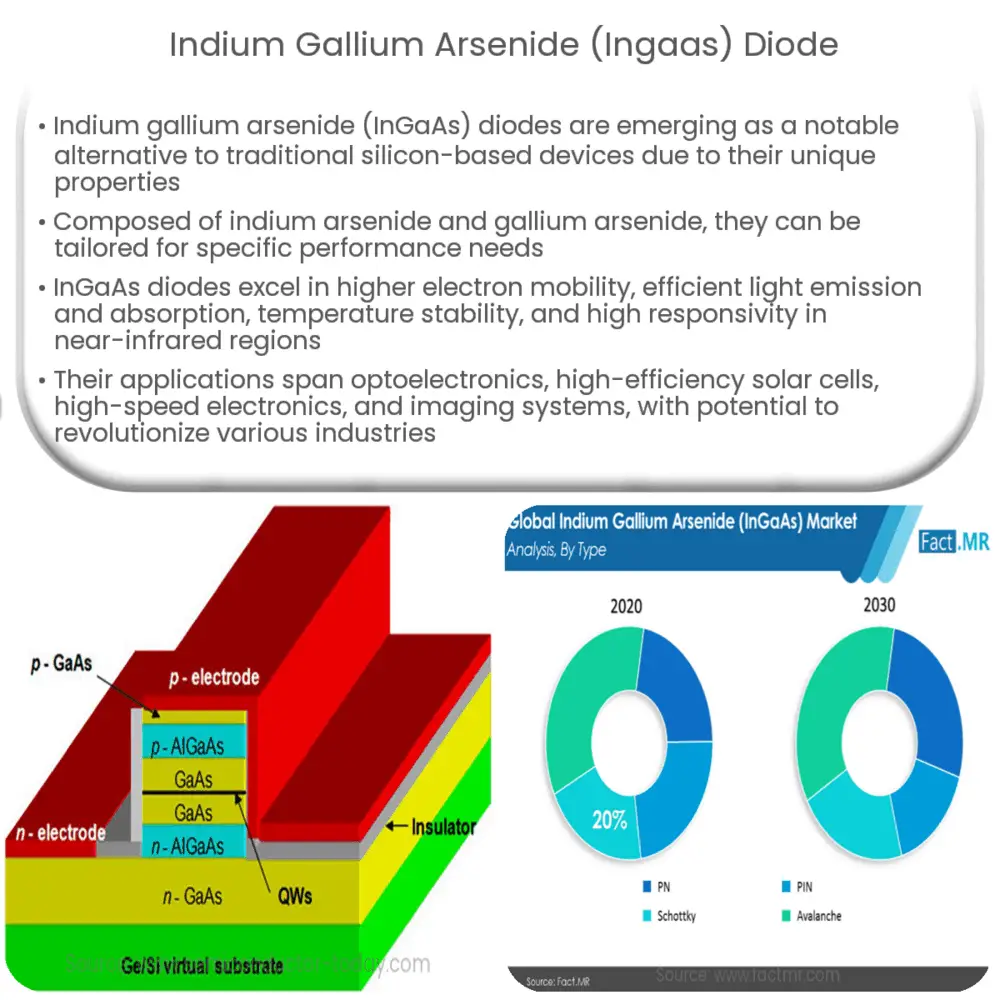
InGaAs diodes are advanced semiconductors with high electron mobility, temperature stability, and excellent optoelectronic properties for various applications.
Indium Gallium Arsenide (InGaAs) Diodes: A Comprehensive Overview
Introduction
Indium gallium arsenide (InGaAs) is a semiconductor material that has been gaining attention in recent years due to its unique properties and wide range of applications. InGaAs diodes are particularly interesting because they offer a number of benefits compared to traditional silicon-based devices. In this article, we will explore the composition, properties, and applications of InGaAs diodes, as well as discuss their potential impact on the future of the electronics industry.
Composition of InGaAs
InGaAs is a ternary compound semiconductor formed by combining indium arsenide (InAs) and gallium arsenide (GaAs). The material’s composition can be tailored by adjusting the ratio of indium to gallium, which in turn alters its properties. This flexibility makes InGaAs an attractive option for many applications, as it can be customized to meet specific performance requirements.
Properties of InGaAs Diodes
InGaAs diodes exhibit several advantageous properties that set them apart from their silicon counterparts. Some of the key properties of InGaAs diodes include:
- Higher Electron Mobility: InGaAs has a higher electron mobility than silicon, which allows for faster signal processing and improved device performance.
- Direct Bandgap: Unlike silicon, InGaAs has a direct bandgap, enabling efficient light emission and absorption. This makes it suitable for use in optoelectronic devices, such as photodetectors and light-emitting diodes (LEDs).
- Temperature Stability: InGaAs diodes have better temperature stability than silicon devices, which means they can maintain performance over a wider range of operating temperatures. This is particularly useful in harsh environments or high-temperature applications.
- High Responsivity: InGaAs photodetectors exhibit high responsivity in the near-infrared region, making them well-suited for telecommunications and sensing applications.
Applications of InGaAs Diodes
Thanks to their unique properties, InGaAs diodes have been employed in a variety of applications, such as:
- Optoelectronics: Due to their direct bandgap, InGaAs diodes are used in optoelectronic devices like photodetectors, lasers, and LEDs. These devices can be found in telecommunication systems, medical equipment, and environmental monitoring systems.
- Solar Cells: InGaAs-based solar cells have shown great promise for increasing the efficiency of photovoltaic devices, particularly in multi-junction solar cells.
- High-Speed Electronics: The high electron mobility of InGaAs allows for the development of high-speed transistors and other electronic devices that outperform their silicon-based counterparts.
- Imaging: InGaAs-based cameras and imaging systems have become increasingly popular in fields such as aerospace, defense, and security due to their ability to detect near-infrared light.
In the second part of this article, we will delve deeper into the fabrication process of InGaAs diodes, as well as explore the challenges and future prospects of this promising semiconductor material.
Fabrication Process of InGaAs Diodes
The fabrication of InGaAs diodes typically involves a series of steps including epitaxial growth, doping, etching, and metallization. One of the most common methods for growing high-quality InGaAs layers is molecular beam epitaxy (MBE), which allows for precise control over the composition and thickness of the material. Alternatively, metal-organic chemical vapor deposition (MOCVD) can be used for large-scale production. Once the InGaAs layer is grown, impurities are introduced through doping to create p-type or n-type regions, which form the basis for diode junctions.
After the epitaxial growth and doping stages, the InGaAs wafer undergoes a series of etching processes to define the diode structures. This can be done using wet chemical etching or dry etching techniques, such as reactive ion etching (RIE). Finally, metal contacts are deposited onto the wafer to establish electrical connections, and the diodes are tested for performance and quality before being packaged and integrated into various electronic systems.
Challenges and Future Prospects
Despite the numerous advantages of InGaAs diodes, there are some challenges associated with their development and use. One major challenge is the cost associated with the fabrication process, as InGaAs wafers are generally more expensive than silicon wafers. Additionally, the integration of InGaAs-based devices with existing silicon-based technology can be complex, requiring innovative solutions to overcome compatibility issues.
Another challenge lies in improving the reliability and efficiency of InGaAs devices. Researchers are continuously working to develop new techniques and materials to further enhance the performance of InGaAs diodes while maintaining cost-effectiveness. These ongoing efforts are expected to drive the widespread adoption of InGaAs diodes in various industries in the coming years.
Looking to the future, InGaAs diodes hold great promise for revolutionizing a wide range of applications. For instance, their use in optoelectronics could significantly improve the speed and efficiency of data transmission in telecommunication networks. Moreover, the development of high-efficiency InGaAs solar cells could help address the growing demand for clean and renewable energy sources. The integration of InGaAs diodes into high-speed electronics and imaging systems could also lead to significant advancements in fields such as aerospace, defense, and security.
Conclusion
In conclusion, InGaAs diodes offer a compelling alternative to traditional silicon-based devices due to their unique properties and wide range of applications. As research continues to advance our understanding of this material and its potential uses, we can expect to see significant growth in the adoption of InGaAs diodes across various industries. By overcoming the existing challenges and capitalizing on the advantages of this promising semiconductor material, InGaAs diodes have the potential to reshape the future of electronics and pave the way for new technological breakthroughs.