CCDs are semiconductor devices that capture and convert light into digital images, offering high resolution, sensitivity, and low noise in various applications.
Charge-Coupled Device (CCD): The Technology Behind Digital Imaging
Charge-coupled devices (CCDs) have revolutionized the world of digital imaging, playing a significant role in various industries, including astronomy, medical imaging, and consumer electronics. Invented in 1969 by Willard S. Boyle and George E. Smith at Bell Labs, CCDs have become an essential component in digital cameras and other imaging devices. In this article, we will explore the underlying technology, key advantages, and limitations of CCDs.
Understanding the Basics of CCDs
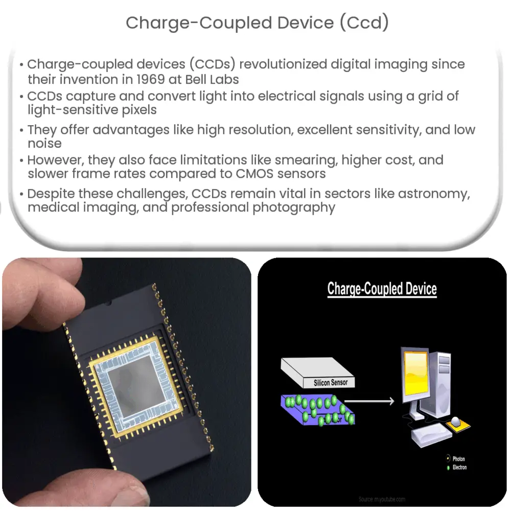
A CCD is a semiconductor device used for capturing and converting light into electrical signals. It is composed of an array of light-sensitive elements, called pixels, which are organized in a grid-like pattern. Each pixel on the CCD corresponds to a single point in the image. When light strikes a pixel, it generates an electrical charge proportional to the intensity of the incoming light. The CCD then measures and stores these charges in a controlled manner to form a digital image.
How CCDs Work: Converting Light to Digital Data
The CCD operates in three primary stages to convert light into digital data: photoelectric effect, charge storage, and charge transfer.
1. Photoelectric Effect
When photons of light interact with the silicon material of the CCD, they generate electron-hole pairs. This process, known as the photoelectric effect, converts light energy into electrical charges. The number of generated charges depends on the intensity and wavelength of the incident light, allowing the CCD to capture variations in color and brightness.
2. Charge Storage
After the photoelectric effect occurs, the electrical charges are stored in the pixel’s potential well. This temporary storage area holds the charges until they can be read and transferred to the output stage. The size of the potential well determines the maximum number of charges a pixel can store, which in turn affects the CCD’s dynamic range and sensitivity.
3. Charge Transfer
The final stage involves the orderly transfer of charges from the pixel array to the output stage. The CCD uses a process called charge-coupling, which shifts the charges row by row and column by column until they reach the output amplifier. The amplifier then converts the charges into voltage signals, which are digitized and processed to form the final digital image.
Key Advantages of CCDs
CCDs offer several benefits over other imaging technologies, such as:
- High Resolution: CCDs can capture images with a high degree of detail, thanks to their densely packed pixel arrays. This makes them ideal for applications requiring high-resolution imaging, such as astronomy and professional photography.
- Excellent Sensitivity: Due to their high quantum efficiency, CCDs can detect even the faintest light signals, allowing them to capture images in low-light conditions.
- Low Noise: CCDs are designed to minimize noise during the charge transfer process, resulting in cleaner, more accurate images.
Limitations of CCDs
Despite their advantages, CCDs also have some limitations that can impact their performance:
- Smearing: During the charge transfer process, charges can accidentally leak into adjacent pixels, causing a distortion known as smearing. This can result in vertical streaks in the final image, particularly when capturing bright light sources.
- Cost and Power Consumption: CCDs tend to be more expensive and consume more power than their counterparts, such as CMOS sensors. This can make them less suitable for battery-operated or cost-sensitive devices.
- Slower Frame Rates: The charge transfer process in CCDs is inherently slower than the parallel readout used in CMOS sensors. Consequently, CCDs typically have lower frame rates, which can be a disadvantage for high-speed imaging applications.
CCD vs. CMOS Sensors
CCDs and CMOS sensors are the two primary types of image sensors used in digital cameras. While both technologies have their strengths and weaknesses, they are suited for different applications:
- CCD: Known for their high resolution, excellent sensitivity, and low noise, CCDs are often preferred for scientific, astronomical, and professional photography applications where image quality is paramount.
- CMOS: CMOS sensors generally offer faster readout speeds, lower power consumption, and lower costs, making them a popular choice for consumer electronics, such as smartphones and action cameras. However, CMOS sensors traditionally had lower image quality compared to CCDs, although advances in technology have significantly narrowed this gap.
Applications of CCDs
Thanks to their ability to capture high-quality images, CCDs have found use in a wide range of applications, including:
- Astronomy: CCDs are extensively used in astronomical telescopes to capture detailed images of celestial objects, even those that emit extremely faint light.
- Medical Imaging: CCDs play a crucial role in medical imaging devices, such as X-ray machines and fluoroscopes, to provide high-resolution images for diagnostic purposes.
- Microscopy: High-resolution CCD cameras are commonly used in microscopy to capture detailed images of microscopic specimens for research and analysis.
- Security Cameras: CCDs are used in surveillance cameras to provide clear and detailed images, which are essential for security purposes.
- Professional Photography: Many high-end digital cameras and DSLRs employ CCDs to deliver superior image quality and performance.
Conclusion
Charge-coupled devices have had a profound impact on the field of digital imaging, offering high resolution, excellent sensitivity, and low noise performance. While they do have some limitations and face competition from CMOS sensors, CCDs continue to be a critical component in a variety of applications where image quality is of utmost importance. As technology advances, we can expect further improvements in CCD performance and even more diverse applications for this versatile imaging technology.
")