Explore the world of Non-contact Electrostatic Force Microscopy: its principles, advantages, applications, challenges, and future perspectives.
Introduction to Non-contact Electrostatic Force Microscopes
The field of microscopy has seen a significant evolution in the past few decades, and one of the most promising developments in this area is the Non-contact Electrostatic Force Microscope (EFM). This powerful tool enables scientists and researchers to examine the electrostatic properties at the nanoscale, which is crucial in various fields, including materials science, nanotechnology, and semiconductor research.
Understanding Non-contact EFM
A non-contact electrostatic force microscope operates on the principle of detecting the electrostatic forces between the tip of the microscope and the sample under investigation. This is fundamentally different from the traditional contact mode Atomic Force Microscopy (AFM), where the tip physically touches the sample surface. Non-contact EFM, as the name suggests, doesn’t require direct contact, which helps to prevent potential damage to the sample or the probe.
Working Principle
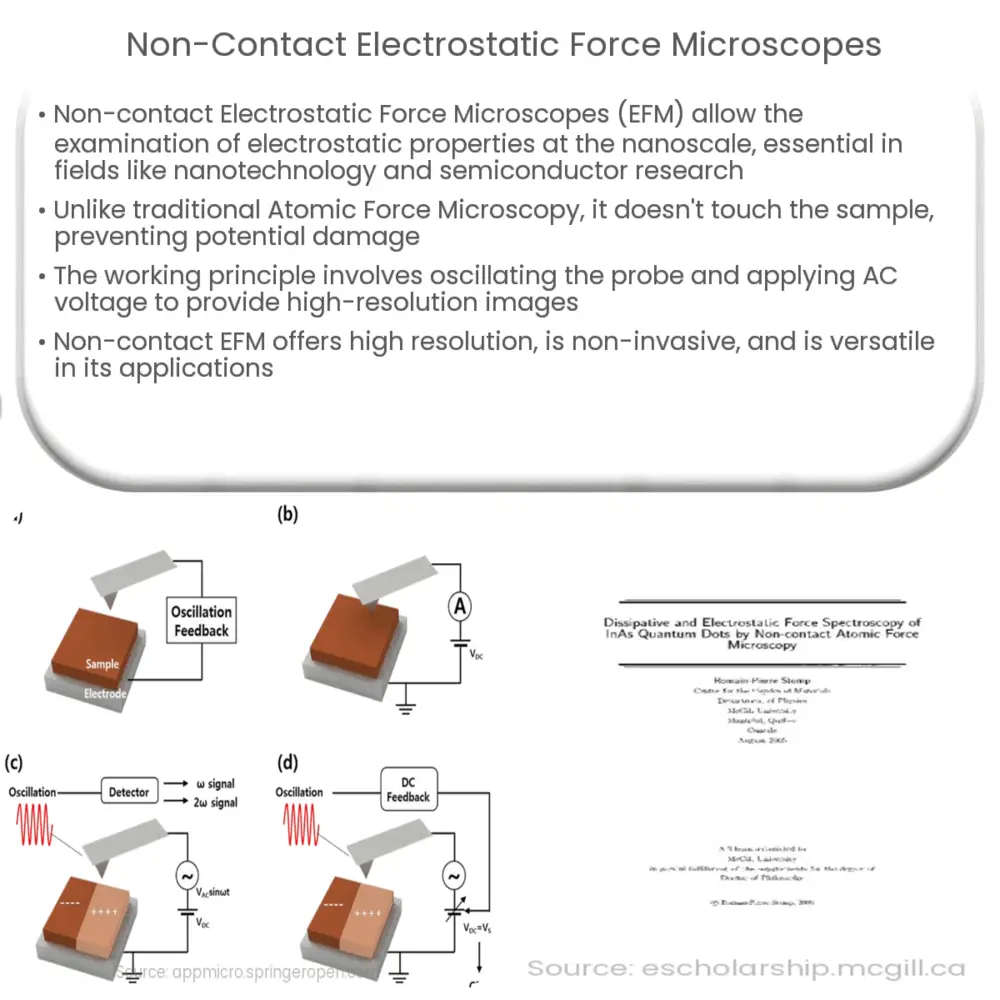
The working principle of a non-contact EFM involves oscillating the probe at a certain frequency above its resonance frequency, maintaining a safe distance from the sample. An AC voltage is applied to the tip, inducing an oscillation in the electrostatic force between the tip and the sample. This causes a change in the resonance frequency of the cantilever, which is detected and mapped to provide high-resolution images of the electrostatic properties of the sample surface.
Advantages of Non-contact EFM
-
High Resolution: Non-contact EFM provides high-resolution images of the electrostatic properties, which is a significant advantage when studying nanoscale materials and structures.
-
Non-Invasive: As no direct contact is made with the sample, the method is non-invasive, preserving the integrity of the sample.
-
Versatility: It can be used on a wide range of materials, including insulators, semiconductors, and even biological samples.
Applications
Due to its versatility and high resolution, non-contact EFM finds application in a multitude of research and industrial sectors. In materials science, it’s used to study the surface potential and charge distribution in materials. In the field of semiconductors, it aids in the inspection of devices at the nanoscale, providing insights into device performance and potential flaws. Furthermore, in biological research, it offers a non-invasive method to study biological samples at the molecular level.
Challenges and Future Perspectives
Despite its many advantages, non-contact EFM is not without its challenges. One of the main difficulties lies in the interpretation of the data, which can be complex due to the multiple forces at play in the interaction between the probe and the sample. Furthermore, the technique requires careful calibration and precise control of the tip-sample distance.
However, ongoing research and development efforts are working to overcome these challenges. Innovations in probe design, signal processing techniques, and advanced algorithms for data interpretation are all promising areas of progress that may enhance the capabilities and ease-of-use of non-contact EFM in the future.
Conclusion
In conclusion, non-contact electrostatic force microscopy represents a significant advance in the field of microscopy. By enabling high-resolution, non-invasive investigation of electrostatic properties at the nanoscale, it opens up new possibilities in a wide range of fields, from materials science and semiconductor research to biological studies. Despite the challenges associated with data interpretation and calibration, the potential benefits of this technique make it a highly valuable tool for both research and industrial applications.
As technology continues to progress and our understanding of the nanoscale world deepens, it’s likely that non-contact EFM will play an increasingly important role in pushing the boundaries of our knowledge and capabilities.