Explore the JTAG (Joint Test Action Group) interface: its history, principles, applications, advantages, limitations, and future trends.
Introduction to JTAG Interfaces
The Joint Test Action Group (JTAG) is a standard interface that has transformed the world of digital systems testing and debugging. It is an integral technology that engineers and developers worldwide have adopted for debugging, programming, and testing purposes on hardware circuits.
Background of JTAG
In the mid-1980s, a global group of microchip manufacturers formed the Joint Test Action Group. Their aim was to develop a method of verifying designs and testing printed circuit boards (PCBs) after manufacture. The result was the IEEE 1149.1 Standard Test Access Port and Boundary-Scan Architecture, commonly referred to as JTAG.
Principles of JTAG
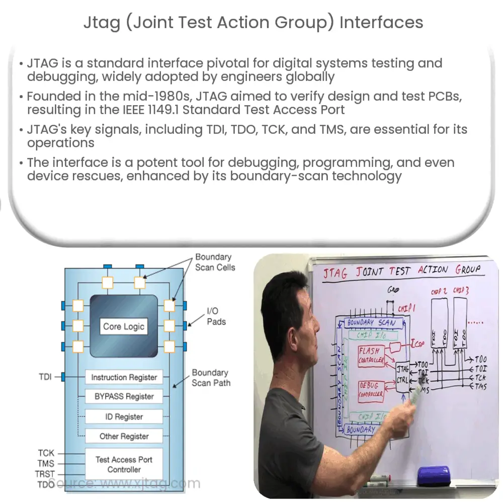
JTAG operates on a set of four key signals: Test Data In (TDI), Test Data Out (TDO), Test Clock (TCK), and Test Mode Select (TMS). These signals constitute the Test Access Port (TAP) that forms the heart of the JTAG interface.
- TDI: This is the input data line. It delivers the instructions and data into the device.
- TDO: This is the output data line. It transmits data from the device to the TAP controller.
- TCK: The clock signal synchronizes the input and output data.
- TMS: This line guides the state machine that controls the operation of the TAP.
Each of these signals plays a critical role in the operation of the JTAG interface.
JTAG in Debugging and Programming
JTAG’s ability to access components on a PCB has made it a powerful tool for debugging and programming. Engineers can manipulate the device’s operations through the JTAG interface, making it an invaluable tool for software debugging and hardware verification.
Furthermore, JTAG’s utility extends beyond testing and debugging. Its in-system programmability makes it suitable for firmware updates, device configuration, and even device rescue operations when other interfaces fail.
Boundary-Scan Technology
One of the key innovations that JTAG introduced is the concept of boundary-scan technology. This involves inserting test cells or “scan cells” at the inputs and outputs of device pins, allowing each pin’s state to be controlled and observed independently. It essentially forms a shift register that loops around the boundary of the device, thus the term ‘boundary-scan’.
JTAG’s Advantages and Limitations
The JTAG interface has proven to be a valuable asset in the electronics industry due to its unique advantages. Its ability to perform in-system programming and debugging, as well as enabling boundary-scan testing, makes it a versatile tool for both software and hardware developers.
However, JTAG is not without limitations. Some devices may lack a JTAG port due to space constraints on the PCB. In addition, the JTAG standard does not define a specific connector or pinout, leading to a lack of uniformity in connector types and potential compatibility issues.
Applications of JTAG
JTAG’s versatility has led to its use in a wide range of applications:
- Hardware debugging: JTAG allows engineers to probe the state of a device at any point in time, providing valuable diagnostic information.
- Firmware updates: The JTAG interface can be used to directly update the firmware on a device.
- Device rescue: When a device becomes unresponsive through its standard interface, JTAG can be used to regain access and potentially repair the device.
- Security: Researchers often use JTAG to uncover vulnerabilities in hardware, aiding in the development of more secure devices.
Future of JTAG
As the complexity of electronic devices continues to increase, the demand for reliable testing and debugging methods like JTAG is expected to grow. Future developments may see enhancements in JTAG’s speed, flexibility, and compatibility, making it an even more powerful tool for engineers and developers.
Conclusion
In conclusion, the Joint Test Action Group (JTAG) interface has revolutionized the way we debug and test digital systems. Despite its limitations, its versatility and widespread use in a variety of applications underscore its importance in the electronics industry. The JTAG interface is likely to remain a valuable tool for debugging, testing, and programming digital systems well into the future.
")

")