Explore the vital role of PCB traces in electronics, their design considerations, types, and impact on device performance.
Introduction to PCB Traces
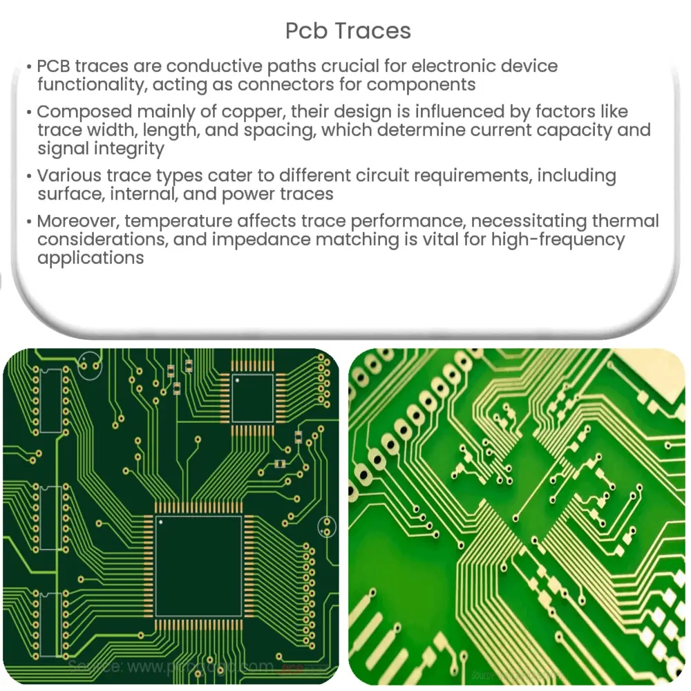
Printed Circuit Board (PCB) traces are one of the most fundamental elements that form the backbone of any electronic device. A PCB trace is simply a conductive path etched onto a PCB that enables the flow of electricity between various points on the board. They serve as the “wiring” that facilitates communication between components, making it possible for the device to function as intended.
The Composition and Functionality of PCB Traces
The primary material used in PCB traces is copper, due to its excellent electrical conductivity and relatively low cost. These copper traces are formed through a process known as etching, wherein a copper-plated board is subjected to a chemical solution that removes the unnecessary copper, leaving only the desired trace pattern.
The function of a PCB trace is quite simple, yet vital. It carries the electrical signal or power from one point to another on the PCB, facilitating the communication between components and enabling the device’s operation. The width, thickness, and length of these traces play a significant role in determining their current carrying capacity, as well as the impedance characteristics.
Factors Influencing PCB Trace Design
When designing a PCB, several factors must be considered to ensure proper trace functionality. These include:
- Trace Width: The width of a trace directly influences its resistance and, by extension, the amount of current it can carry. Thicker traces can carry more current without overheating.
- Trace Length: The length of a trace has a profound impact on signal integrity. Longer traces may result in signal delay or attenuation.
- Trace Spacing: Trace spacing is crucial in preventing crosstalk between adjacent traces. The greater the spacing, the lesser the interference.
These considerations help ensure the PCB performs as desired and is robust enough to withstand the electrical demands of the device it supports.
Types of PCB Traces
PCB traces are not one-size-fits-all. There are several types, each designed to fulfill specific requirements:
- Surface Traces: These are located on the outer layers of the PCB. They are most common and easiest to design and manufacture.
- Internal Traces: Located inside the PCB, these traces are used when the complexity of the circuit increases.
- Power or Ground Planes: These are wide areas of copper on a PCB, used for carrying power or grounding signals.
Understanding the Impact of Temperature on PCB Traces
Temperature plays a crucial role in the performance of PCB traces. As the temperature increases, the resistance of the copper trace also increases, which can lead to a reduction in the current-carrying capacity. Hence, understanding the thermal properties and providing adequate cooling mechanisms are critical for the optimal functioning of PCBs.
PCB Trace Antennas
An interesting application of PCB traces is seen in the creation of trace antennas. Also known as printed antennas, these are antennas that are formed by a conducting trace on the PCB. They are extensively used in wireless communication devices due to their low cost, ease of integration into circuits, and good performance.
PCB Trace Impedance Matching
Impedance matching is a crucial factor in PCB trace design, especially in high-frequency applications. When the trace impedance is not matched to the source and load impedance, it can lead to signal reflection, causing distortion and potential loss of data. Thus, impedance control is a key element in PCB design.
Conclusion
In conclusion, PCB traces are an integral part of any electronic device, acting as the vital connectors that enable communication between components. From their composition to design considerations, types, and applications, each aspect of a PCB trace plays a significant role in the performance and efficiency of the final product.
The design of PCB traces calls for an understanding of various parameters such as width, length, spacing, temperature, and impedance matching. Adhering to best practices in trace design can greatly improve signal integrity, reduce interference, and enhance overall device performance.
Whether it’s a simple device or a complex piece of technology, it’s the humble PCB traces that bring life to the concept, facilitating the functionality we often take for granted. They truly form the lifeline of modern electronic devices.