Explore FinFET technology, its unique design, advantages over traditional transistors, challenges, and its future prospects in microelectronics.
Understanding FinFET Technology
The relentless pursuit of enhanced performance and energy efficiency in integrated circuits has driven the continuous miniaturization of transistor dimensions, commonly referred to as Moore’s Law. As the scale of these devices approaches the atomic level, conventional transistor designs encounter severe challenges. To overcome these limitations, an innovative technology known as Fin Field-Effect Transistor (FinFET) has been introduced.
What is FinFET?
FinFET is a type of non-planar or “3D” transistor that is used in the design of modern processors. As a subtype of MOSFET (Metal-Oxide-Semiconductor Field-Effect Transistor), FinFET takes its name from the thin, fin-like structure that extends above the surface of the substrate.
Design and Operation of FinFET
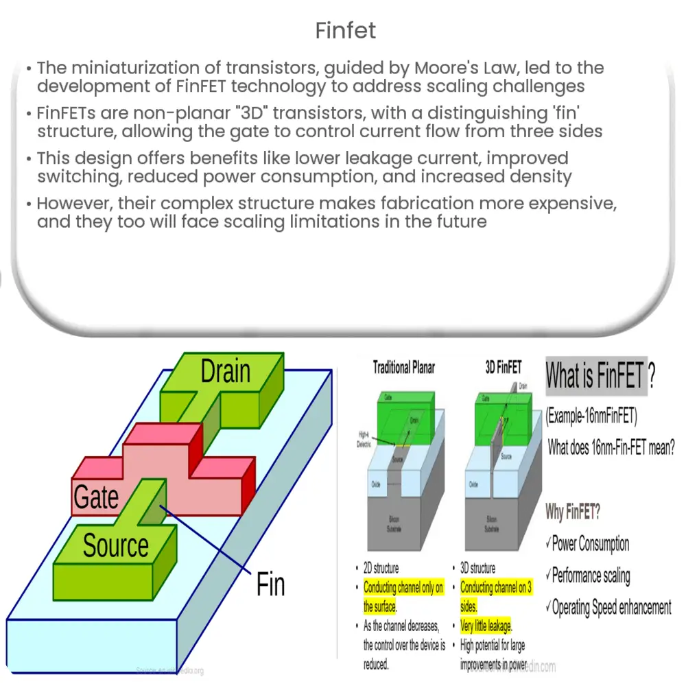
The FinFET design is distinct from that of a planar transistor. Its key feature is the ‘fin’, a thin silicon structure that rises above the substrate, on which the gate material is deposited. Unlike in traditional planar designs, the gate material surrounds the fin on three sides, hence often referred to as a ‘trigate’ design. This design allows for better control over the current flow through the channel, enhancing performance and reducing leakage.
- Source and Drain: These two terminals are located at either end of the fin. They act as the entry and exit points for the electrons during operation.
- The Fin: This is the thin vertical silicon structure that rises above the substrate. The fin determines the thickness of the channel through which the electrons flow.
- The Gate: This is the terminal that controls the flow of current through the channel. In a FinFET, the gate is wrapped around three sides of the fin, giving it greater control over the current flow.
In operation, applying a voltage to the gate creates an electric field that modulates the conductivity of the channel. This in turn allows the FinFET to function as a switch, controlling the flow of electrons from the source to the drain.
Benefits of FinFET Technology
FinFET technology offers several benefits over traditional planar transistor design. These advantages primarily stem from its ability to mitigate short-channel effects, which become more pronounced as devices continue to scale down in size. Short-channel effects can lead to increased power consumption and decreased performance, issues that FinFET can effectively address.
Specific Advantages of FinFET Technology
- Lower Leakage Current: Due to the three-dimensional gate structure, a FinFET can exert better control over the channel, reducing leakage current.
- Improved Switching Performance: The enhanced control over the channel also enables faster switching, improving overall performance.
- Lower Power Consumption: By reducing leakage and improving switching, FinFETs can significantly lower power consumption, making them ideal for battery-powered devices.
- Increased Density: FinFETs can be packed more densely than planar transistors, which is a critical requirement for the continued miniaturization of integrated circuits.
Challenges and Future Prospects
Despite these significant advantages, FinFET technology is not without challenges. For instance, the three-dimensional structure makes fabrication more complex and costly. Additionally, as device dimensions continue to shrink, even FinFETs will eventually encounter physical and performance limitations.
Nevertheless, the industry has adopted FinFET technology for advanced process nodes, and it will likely remain the dominant transistor design for several years. Researchers are exploring novel transistor designs such as nanowire FETs and gate-all-around (GAA) FETs to eventually succeed FinFETs.
Conclusion
In conclusion, FinFET technology represents a significant evolution in transistor design, offering enhanced performance, lower power consumption, and increased packing density over traditional planar transistors. Despite the challenges associated with their fabrication, FinFETs have become an essential component of modern integrated circuits, enabling the continued miniaturization of electronic devices in accordance with Moore’s Law. As we look to the future, the lessons learned from the adoption of FinFETs will undoubtedly inform the development and deployment of even more advanced transistor technologies.